


The Hardware Enablers for the Internet of Things – Part II (More than Moore)
Part I of this two-part series on "The Hardware Enablers for the Internet of Things," introduced how CMOS semiconductor devices enable wireline and wireless communications at what is commonly called the Physical Layer (PHY). The density of digital circuits (CPU, memory, I/O) has been increasing as the critical dimensions such as gate length and minimum feature half pitch have been scaled down by a factor of two every 18 months.
This observation is attributed to Gordon Moore who first described it in 1965 and in his paper entitled, "Cramming More Components onto Integrated Circuits" found in the Proceedings Of The IEEE, VOL. 86, NO. 1, January 1998.
Since 1998, the International Technology Roadmap for Semiconductors (ITRS) has served as compass to guide the industry by predicting technology trends and publicizing the need for industry standards, processing equipment requirements, and market drivers. The International Roadmap Committee (IRC) and 16 technology working groups meet regularly for workshops and symposia to publish and release an ITRS Roadmap every two years. The roadmap provides a benchmark for the semiconductor industry and helps to set the priorities for research and development. The road to "More Moore" has successfully scaled Complementary Metal-Oxide Semiconductor (CMOS) devices and interconnects to achieve better speed, lower power, smaller size and higher yields; resulting in today’s FinFET, FD-SOI, High-k, Low-k and SiGe technology. For the last 25 years, CMOS scaling has followed this law. In 1995, gate feature size was 250nm; today it is 22nm. By 2025, photolithography scaling may hit the limit at ~ 5nm. Recently, IHP (Germany) and GaTech (USA) reported at a SiGe transistor that operates at 0.8 THz, which is thought to be the territory of III-V devices. After "More Moore" efforts are exhausted, new technologies and materials to overcome this "wall" are needed. Research areas for "Beyond CMOS" now include integration of III-V materials, graphene, silicene, nano-wire transistors, quantum dots, NEMS and spintronics. But many of these innovations may never come into fruition or may take decades before entering the commercial mainstream.
More than Moore
In the 2005, ITRS addressed the potential ending of the scaling for CMOS and recommended a roadmapping for "More than Moore" (MtM) as forks in the road in the now famous diagram shown below:
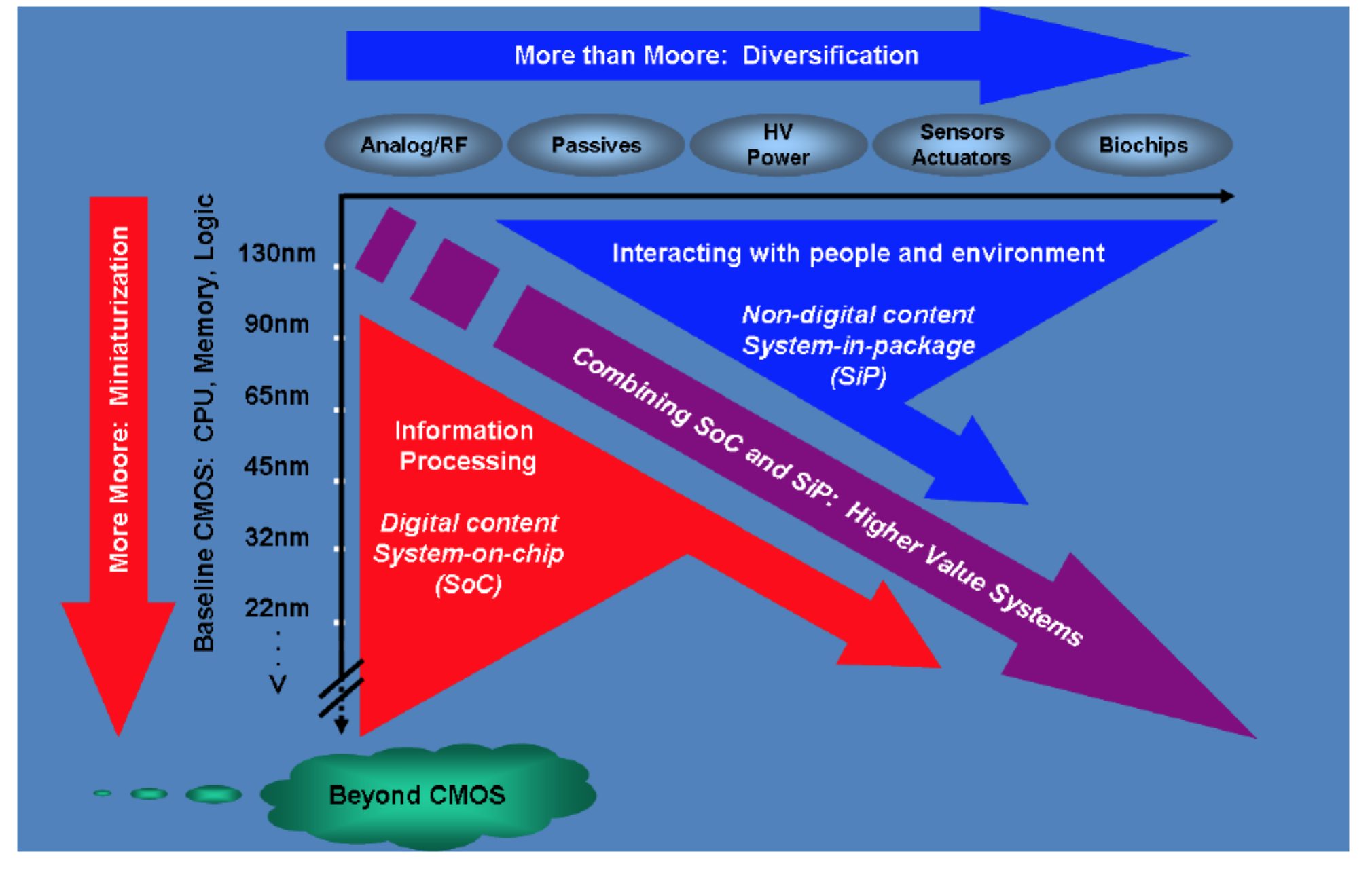
The combined need for digital and non-digital functionalities in an integrated system
Clearly, data processing and memory will continue down a path of "More Moore"” and eventually be replaced by "Beyond CMOS" technologies. Digital processing is well suited for higher and higher integration for a System-on-chip (SoC) realization. But in turns of sensor, actuators, analog/RF and passives, ITRS shows a different path – the path we now commonly call "More than Moore" since their performance improvements do not scale according to Moore’s Law.
Mart Graef has written and presented "Positioning More than Moore Characterization Needs and Methods within the ITRS" in 2011. The paper and presentation slides are excellent resources.
It is indeed not a coincidence that the concept of the Internet of Things started to become popular at about the same time as the 2005 ITRS report. The five devices types identified for More than Moore designation are all enabling PHY level hardware whose advancement are critical for the IoT eco-systems to become a reality. The remainder of this article addresses some aspects and challenges for each one of them: Analog/RF, Passives, HV Power, Sensor/Actuators and Biochips.
With the lower voltages associated with each new generation of advanced CMOS, the performance of many analog/RF circuits are degraded (lower noise margins, lower linearity and reduced output power). Therefore III-V devices and circuits based on gallium arsenide (GaAs) and gallium nitride (GaN) still play a dominant role in the RF front-end chipsets for many wireless radios required for IoT. GaN devices can achieve operating voltages in the 28V to 48V range while delivering 5 to 10 W/mm power densities. III-V devices can easily support millimeter-wave operations (≥ 60 GHz). If the transmit/receive range is very short (<100m), Si CMOS or SiGe RFICs are sufficiently capable.
Passives in the form of capacitors, inductors, and resistors can be realized as thin-film or packaged for SMT attachment. In a typical electronics assembly or board, the passive components can account for greater than 60% of the PWB area and 80% of the Build of Material (BOM) device count. Reduction in passives is a challenge for small IoT devices.
High voltage power devices are needed to provide power management, regulation and conversion of system power supply voltages down to the much lower terminal voltages for the IC transistors. Traditionally, Si MOSFET and diodes has been the workhorse devices for such power electronics. More recently, GaN and SiC devices have emerged as potential technology to make smaller DC-DC converters.
Getting smart
Without Micro Electro-mechanical Systems (MEMS) and Sensors, the "Smart" in "Smart Devices" for IoT applications cannot be realized. Sensor and actuators perform as accelerometers, gyroscopes, image sensors, humidity sensor, microphones, pressure sensors, proximity sensors, and temperature sensors, touchscreen interfaces and switches. Sensors/actuators also do not follow Moore’s Law. To interact with the physical environment and people, making circuits smaller is neither required nor practical. The human to machine interface should be sized appropriately to meet the human geometries. For informative descriptions of various MEMS and sensor devices, the STMicro website, Bosch website and Freescale website are good resources.
Biochips will enable IoT applications in the area of personalized advanced healthcare, home diagnostic kits, healthcare monitoring and the low-cost collection of medical data shared with the patient’s health care providers through the cloud. IMEC has been a key researcher of biochips for IoT and wearable applications. Professor John Rogers, University of Illinois, Urbana-Champaign, will be giving a plenary talk, "Soft Assemblies of Radios, Sensors and Circuits for the Skin" at the MTT-S IMS2015 conference scheduled for 18 May 2015. Consumer product companies like Samsung and Apple are also investing heavily into IoT/Wearable devices for health and fitness monitoring.
ITRS has identified that the key technology to tie all the MtM and More Moore devices together as System in Package (SiP). Although each of the functions may be implemented in separate technologies or technology nodes, they can be integrated into a very small microsystem through wafer-level integration and chip stacking. For an example, see the EE Times article on a Bluetooth SiP module that enables IoT applications.
For further reading, I recommend that you download Wolfgang Arden’s "More-than-Moore" White Paper, read M. Brillouët’s “Towards a ‘More-than-Moore’ Roadmap” and P. Gargini’s presentation.
 Timothy Lee is the 2015 IEEE Microwave Theory and Techniques Society (MTT-S) President. Currently he is a Boeing Technical Fellow, working in Boeing Research and Technology in Southern California. He has over 35 years' experience in the design of MMICs, microwave components and sub-systems for electronic systems. His interests in IEEE MTT-S include the continued excellence of technical journals and conferences for the microwave engineering communities worldwide and the development of microwave/wireless solutions to benefit humanitarian needs.
Sign Up for IoT Technical Community Updates
Calendar of Events
IEEE 8th World Forum on Internet of Things (WF-IoT) 2022
26 October-11 November 2022
Call for Papers
IEEE Internet of Things Journal
Special issue on Towards Intelligence for Space-Air-Ground Integrated Internet of Things
Submission Deadline: 1 November 2022
Special issue on Smart Blockchain for IoT Trust, Security and Privacy
Submission Deadline: 15 November 2022
Past Issues
September 2022
July 2022
March 2022
January 2022
November 2021
September 2021
July 2021
May 2021
March 2021
January 2021
November 2020
July 2020
May 2020
March 2020
January 2020
November 2019
September 2019
July 2019
May 2019
March 2019
January 2019
November 2018
September 2018
July 2018
May 2018
March 2018
January 2018
November 2017
September 2017
July 2017
May 2017
March 2017
January 2017
November 2016
September 2016
July 2016
May 2016
March 2016
January 2016
November 2015
September 2015
July 2015
May 2015
March 2015
January 2015
November 2014
September 2014